- 您现在的位置:买卖IC网 > Sheet目录328 > IDT7034L20PFI (IDT, Integrated Device Technology Inc)IC SRAM 72KBIT 20NS 100TQFP
IDT7034S/L
High-Speed 4K x 18 Dual-Port Static RAM
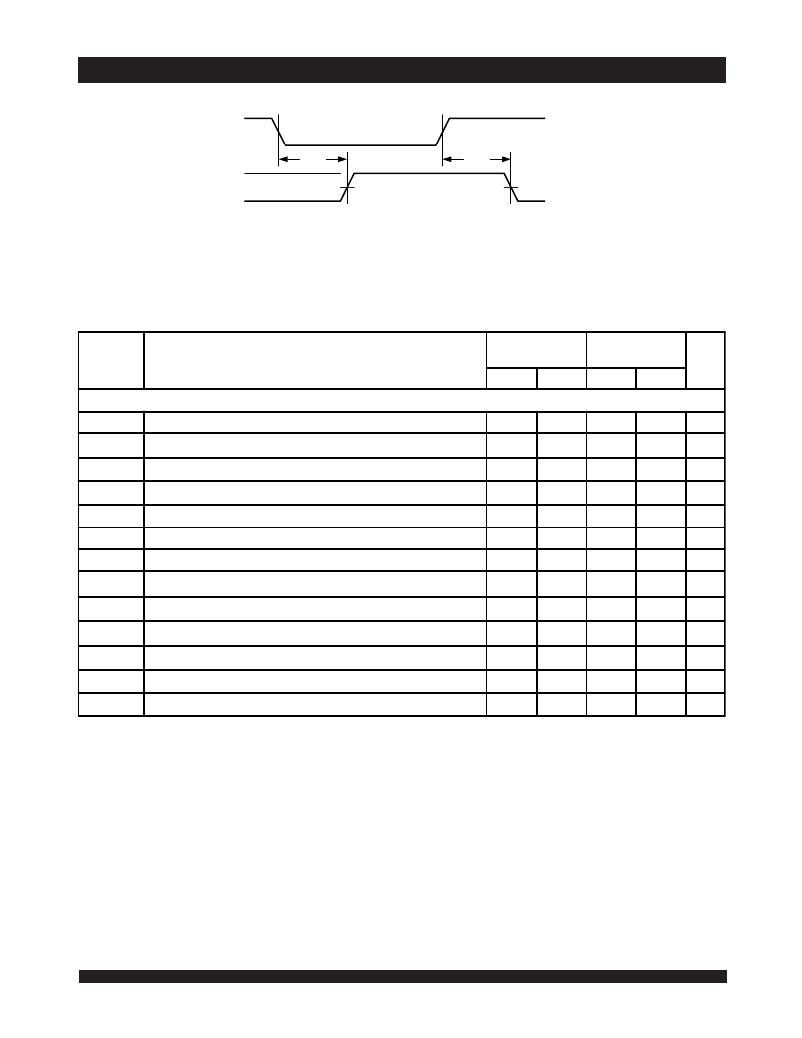
Timing of Power-up Power-down
CE
t PU
I CC
50%
I SB
Industrial and Commercial Temperature Ranges
t PD
50%
AC Electrical Characteristics Over the
Operating Temperature and Supply Voltage (5)
4089 drw 06
,
7034X15
Com'l Only
7034X20
Com'l & Ind
Symbol
Parameter
Min.
Max.
Min.
Max.
Unit
WRITE CYCLE
t WC
t EW
t AW
t AS
t WP
t WR
t DW
t HZ
t DH
t WZ
t OW
t SWRD
t SPS
Write Cycle Time
Chip Enable to End-of-Write (3)
Address Valid to End-of-Write
Address Set-up Time (3)
Write Pulse Width
Write Recovery Time
Data Valid to End-of-Write
Output High-Z Time (1,2)
Data Hold Time (4)
Write Enable to Output in High-Z (1,2)
Output Active from End-of-Write (1,2,4)
SEM Flag Write to Read Time
SEM Flag Contention Window
15
12
12
0
12
0
10
____
0
____
0
5
5
____
____
____
____
____
____
____
10
____
10
____
____
____
20
15
15
0
15
0
15
____
0
____
0
5
5
____
____
____
____
____
____
____
12
____
12
____
____
____
ns
ns
ns
ns
ns
ns
ns
ns
ns
ns
ns
ns
ns
NOTES:
4089 tbl 13
1. Transition is measured 0mV from Low or High-impedance voltage with the Output Test Load (Figure 2).
2. This parameter is guaranteed by device characterization, but is not production tested.
3. To access RAM, CE = V IL , UB or LB = V IL , SEM = V IH . To access semaphore, CE = V IH or UB & LB = V IH , and SEM = V IL . Either condition must be valid for the entire
t EW time.
4. The specification for t DH must be met by the device supplying write data to the RAM under all operating conditions. Although t DH and t OW values will vary over voltage and
temperature, the actual t DH will always be smaller than the actual t OW .
5. 'X' in part numbers indicates power rating (S or L).
8
发布紧急采购,3分钟左右您将得到回复。
相关PDF资料
IDT7035L20PFI
IC SRAM 144KBIT 20NS 100TQFP
IDT7037L20PFI
IC SRAM 576KBIT 20NS 100TQFP
IDT7038L15PFG
IC SRAM 1024KBIT 15NS 120TQFP
IDT7052L20G
IC SRAM 16KBIT 20NS 108PGA
IDT7054L20G
IC SRAM 32KBIT 20NS 108PGA
IDT709089L9PF
IC SRAM 512KBIT 9NS 100TQFP
IDT709099L9PFI
IC SRAM 1MBIT 9NS 100TQFP
IDT709149S10PFI
IC SRAM 36KBIT 10NS 80TQFP
相关代理商/技术参数
IDT7034L20PFI8
功能描述:IC SRAM 72KBIT 20NS 100TQFP RoHS:否 类别:集成电路 (IC) >> 存储器 系列:- 标准包装:72 系列:- 格式 - 存储器:RAM 存储器类型:SRAM - 同步 存储容量:9M(256K x 36) 速度:75ns 接口:并联 电源电压:3.135 V ~ 3.465 V 工作温度:-40°C ~ 85°C 封装/外壳:100-LQFP 供应商设备封装:100-TQFP(14x14) 包装:托盘 其它名称:71V67703S75PFGI
IDT7034S15PF
功能描述:IC SRAM 72KBIT 15NS 100TQFP RoHS:否 类别:集成电路 (IC) >> 存储器 系列:- 标准包装:45 系列:- 格式 - 存储器:RAM 存储器类型:SRAM - 双端口,异步 存储容量:128K(8K x 16) 速度:15ns 接口:并联 电源电压:3 V ~ 3.6 V 工作温度:0°C ~ 70°C 封装/外壳:100-LQFP 供应商设备封装:100-TQFP(14x14) 包装:托盘 其它名称:70V25S15PF
IDT7034S15PF8
功能描述:IC SRAM 72KBIT 15NS 100TQFP RoHS:否 类别:集成电路 (IC) >> 存储器 系列:- 标准包装:72 系列:- 格式 - 存储器:RAM 存储器类型:SRAM - 同步 存储容量:9M(256K x 36) 速度:75ns 接口:并联 电源电压:3.135 V ~ 3.465 V 工作温度:-40°C ~ 85°C 封装/外壳:100-LQFP 供应商设备封装:100-TQFP(14x14) 包装:托盘 其它名称:71V67703S75PFGI
IDT7034S20PF
功能描述:IC SRAM 72KBIT 20NS 100TQFP RoHS:否 类别:集成电路 (IC) >> 存储器 系列:- 标准包装:45 系列:- 格式 - 存储器:RAM 存储器类型:SRAM - 双端口,异步 存储容量:128K(8K x 16) 速度:15ns 接口:并联 电源电压:3 V ~ 3.6 V 工作温度:0°C ~ 70°C 封装/外壳:100-LQFP 供应商设备封装:100-TQFP(14x14) 包装:托盘 其它名称:70V25S15PF
IDT7034S20PF8
功能描述:IC SRAM 72KBIT 20NS 100TQFP RoHS:否 类别:集成电路 (IC) >> 存储器 系列:- 标准包装:72 系列:- 格式 - 存储器:RAM 存储器类型:SRAM - 同步 存储容量:9M(256K x 36) 速度:75ns 接口:并联 电源电压:3.135 V ~ 3.465 V 工作温度:-40°C ~ 85°C 封装/外壳:100-LQFP 供应商设备封装:100-TQFP(14x14) 包装:托盘 其它名称:71V67703S75PFGI
IDT7035L15PF
功能描述:IC SRAM 144KBIT 15NS 100TQFP RoHS:否 类别:集成电路 (IC) >> 存储器 系列:- 标准包装:1,000 系列:- 格式 - 存储器:RAM 存储器类型:SRAM - 双端口,同步 存储容量:1.125M(32K x 36) 速度:5ns 接口:并联 电源电压:3.15 V ~ 3.45 V 工作温度:-40°C ~ 85°C 封装/外壳:256-LBGA 供应商设备封装:256-CABGA(17x17) 包装:带卷 (TR) 其它名称:70V3579S5BCI8
IDT7035L15PF8
功能描述:IC SRAM 144KBIT 15NS 100TQFP RoHS:否 类别:集成电路 (IC) >> 存储器 系列:- 标准包装:45 系列:- 格式 - 存储器:RAM 存储器类型:SRAM - 双端口,异步 存储容量:128K(8K x 16) 速度:15ns 接口:并联 电源电压:3 V ~ 3.6 V 工作温度:0°C ~ 70°C 封装/外壳:100-LQFP 供应商设备封装:100-TQFP(14x14) 包装:托盘 其它名称:70V25S15PF
IDT7035L20PF
功能描述:IC SRAM 144KBIT 20NS 100TQFP RoHS:否 类别:集成电路 (IC) >> 存储器 系列:- 标准包装:45 系列:- 格式 - 存储器:RAM 存储器类型:SRAM - 双端口,异步 存储容量:128K(8K x 16) 速度:15ns 接口:并联 电源电压:3 V ~ 3.6 V 工作温度:0°C ~ 70°C 封装/外壳:100-LQFP 供应商设备封装:100-TQFP(14x14) 包装:托盘 其它名称:70V25S15PF
